If you’ve ever worked on a prototype PCB, you know the moment the first assembled board hits your lab bench—part of you is excited, part of you is crossing your fingers it works, and all of it hinges on how we placed the parts. I’ve been running a prototype PCB assembly shop for over 12 years, and let me tell you: no two prototype projects are the same, so we don’t use a one-size-fits-all approach for component placement. Today I’m breaking down exactly what techniques we lean on, why each matters, and how they make or break a prototype’s ability to go from sketchy breadboard to functional, testable sample. Prototype PCB Assembly

First, let’s ground this: prototypes aren’t mass production. When we’re doing a prototype run, we’re not cranking out 10,000 identical boards to sell—we’re building 1 to 50 boards for a startup, an engineer, a lab, maybe a hobbyist who just landed their first big project. That means our component placement techniques have to be flexible, fast, and forgiving for the inevitable last-minute design tweaks that come with prototyping. No rigid JIGs here; we adapt to your schematic, not the other way around.
1. Pick-and-Place with Fine-Tuned Manual Override (Our Go-To for Most Prototypes)
You’ve probably heard of pick-and-place machines—they’re the big, automated arm systems that grab parts from reels and plop them on PCBs super fast. For prototype work, we don’t just hit “go” and walk away. Our pick-and-place is tuned for small, odd-ball parts (think 0201 resistors, tiny SMD capacitors, or weird custom ICs) that aren’t always on standard reels, and here’s the secret weapon: we turn on manual override for everything pre-production.
Wait, why not full automation? Prototypes often have unique component footprints. Last quarter we had a startup come to us with a custom RF IC that wasn’t in any of our standard pick-and-place libraries. Instead of forcing a bad fit that would short out, our tech manually aligned each IC using a microscope and the machine’s fine-adjustment tool. That would be a nightmare for mass production—too slow, too expensive—but for prototypes, it’s exactly what lets us keep costs low while getting accurate placement. We also leave a tiny bit of extra space around through-hole parts (even though most prototypes use SMD) so if the engineer needs to tweak traces or add a jumper late, they don’t have to desolder parts to make room.
Pro tip from our shop: If your prototype has parts with tight pitch (like 0.5mm QFNs), we test the placement with a quick visual check under magnification before soldering the whole board. No skipping that step—we’ve seen too many prototypes fail because a pick-and-place machine shifted a part 0.1mm that didn’t show up until testing.
2. Manual Placement for One-Off, Super Small Prototypes
If you’re making a single board—say, a test sensor for a university lab—automation is overkill. We keep a dedicated workbench for manual component placement, stocked with all the stuff you need: fine-tipped tweezers, flux pens, hot air pencils, and magnifying lamps. Our techs have been doing this for years, so they can place a 0402 resistor by hand in 2 seconds, no problem.
When do we use this? Typically for projects with less than 50 total parts, or when the PCB itself is tiny (like a credit card or smaller). It’s way faster to set up a manual workbench than calibrate a pick-and-place for 10 boards, and it’s cheaper for the customer. Last month we had a customer who only needed 2 test boards for a new wearable—they couldn’t afford the setup fee for a small pick-and-place run, so we did everything by hand for half their projected prototype budget. The catch here? We add a little buffer for human error, so we always have extra parts on hand for this work. No one wants to wait a week for a replacement 0402 capacitor because we dropped it mid-placement.
3. Heat Map and Flow-Based Placement for Functional Prototypes
Once the component list is locked (or mostly locked—prototype designs always change), we use flow-based placement to group parts that need to work together. For example, if you have an MCU that sends data to an LCD, we place the LCD as close to the MCU as possible to cut down on signal noise. If you have a power supply section, we group all capacitors and regulators near the power input to keep traces short.
But here’s the other big part: thermal placement. If your prototype has a power IC or a microcontroller that runs hot, we don’t just plop it anywhere. We use a simple heat map (we run a quick simulation before placement) to put high-heat parts where they have the most airflow, and away from sensitive parts that hate heat. Last year we had a drone startup come to us with a prototype that kept overheating because their ESC was placed right next to the GPS module—signal interference AND heat killing their test flights. We swapped their placement in 10 minutes, and their next test flight worked perfectly. This technique isn’t just for performance—it saves customers from wasting weeks debugging a board that has avoidable placement issues.
4. Through-Hole Hybrid Placement for Prototype Boards with Mixed Parts
A lot of prototype projects aren’t all SMD. Some engineers still use through-hole parts for big connectors (like USB ports or power jacks) that are easier to solder by hand, or for high-power components that need extra structural support. So we do hybrid placement: we place all SMD parts first with pick-and-place, then add through-hole parts by hand, making sure we don’t accidentally knock any SMD parts loose when handling the board.
Wait, but why not just use all through-hole? Because SMD parts are smaller, faster, and cheaper for most modern prototypes. But hybrid placement gives customers the best of both worlds: they get the miniaturization of SMD for most parts, and the robustness of through-hole for connectors that get plugged and unplugged all the time. We also leave a little extra space around through-hole connectors so if the customer needs to add a custom wire or jumper later, they don’t have to desolder the connector to make room. That’s a huge win for prototyping, where testing often leads to quick changes.
5. Flexible Jig Placement for Reproducible Small Batches of Prototypes
If a customer needs 10 or 20 boards (not just 1 or 50), we make a custom flexible jig for placement. These aren’t the heavy, expensive JIGs used for mass production—they’re 3D-printed, lightweight, and super cheap to make. The jig has holes or cutouts that match the PCB’s mounting points, so when we press the board into the jig, it’s perfectly aligned every single time. Then we use pick-and-place or manual tools to put parts where they need to go.
This solves a big prototype problem: if you need multiple identical boards, how do you make sure the parts are in the exact same spot every time? Without a jig, even a tiny shift in placement can lead to one board working and another failing. For a startup that’s testing 10 boards for market research, consistency is key. We’ve had customers come back after their first small batch and ask for another 10 boards that work exactly the same—jig placement lets us do that without re-calibrating the entire pick-and-place machine for every run.
Now, let’s talk about what we never do for prototypes. We skip overcomplicated placement rules that apply to mass production, like optimizing for 10,000 boards worth of soldering time. For prototypes, we prioritize testability first. That means we leave test points in easy-to-reach spots, we don’t crowd parts so you can probe them with a multimeter, and we label every component spot if you want. We know that a prototype is supposed to be tested, tweaked, and reworked—so our placement is designed to make that easy, not hard.
At the end of the day, the best component placement technique for your prototype is the one that fits your project’s needs. If you need a single board for a university lab, manual placement is perfect. If you need 20 identical boards for a startup’s first field test, flexible jig placement is the way to go. If you have weird, custom parts, fine-tuned pick-and-place with manual override is our jam.
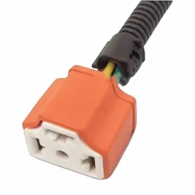
If you’re working on a prototype PCB project, no matter how big or small, we can help figure out the right placement approach for you. We don’t do cookie-cutter prototype assembly—we adjust to your schematic, your timeline, and your budget. Reach out to talk through your project, and let’s build a prototype that works the first time you test it.
References
Automotive Wire Harness IPC-7351, Generic Requirements for Surface Mount Design and Land Pattern Standard
NXP Semiconductors, “Prototype PCB Assembly Best Practices for High-Volume Transition”
Journal of Electronic Manufacturing, “Component Placement Strategies for Rapid Prototyping”
IPC-D-317, Design Standard for Electronic Assemblies
Huaswin Electronics Technology Co., Ltd.
Address: Building A2, Hao Hai Hong Industrial Park, No.3 Yu He Road, Gong He, Sha Jing, Bao An, Shenzhen
E-mail: sales@huaswin.com
WebSite: https://www.huaswin-pcba.com/
